I2C
1 Function Overview
The I2C interface can be connected to the I2C or SMBus bus through the data pin (SDA) and clock pin (SCL). Both SDA and SCL lines are set as open-drain outputs and are connected to pull-up resistors. Therefore, multiple devices can be mounted on the I2C and SMBus buses. Each I2C interface transmission is initiated and controlled by the master device
This chapter mainly introduces the completion of data read and write operations on the EEPROM chip through the I2C interface. Currently, the CP side does not allow the use of I2C, while the AP side supports the use of I2C0 and I2C1.
For theoretical introduction to I2C, refer to: I2C_driver
Note
1.The CP side does not allow the use of I2C0 and I2C1;
2.The AP side supports the use of I2C0 and I2C1;
2 code path
- demo_path:
components\bk_cli\cli_i2c.c
- driver_source_code_path:
ap\middleware\driver\i2c\i2c_unified.c(Unified API layer, automatically routes to hardware or simulated I2C)ap\middleware\driver\i2c\i2c_driver.c(Hardware I2C driver implementation)ap\middleware\driver\i2c\sim_i2c_driver.c(Software simulated I2C driver implementation)
Note
1.i2c_unified.c: Unified API layer that automatically routes to hardware or simulated I2C based on I2C ID
2.i2c_driver.c: Hardware I2C driver implementation using hardware interrupts
3.sim_i2c_driver.c: Software simulated I2C driver implementation via GPIO timing simulation
3 cli Command Overview
Demo Running Dependencies: Macro Configuration
NAME
Description
File
value
CONFIG_I2C
support i2c
ap\middleware\soc\bk7236\bk7236.defconfigy
CONFIG_I2C_SUPPORT_ID_BITS
support i2c0 or i2c1
ap\middleware\soc\bk7236\bk7236.defconfig1
CONFIG_SIM_I2C
value y:support software; n: hardware i2c
ap\middleware\soc\bk7236\bk7236.defconfign
CONFIG_SIM_I2C_HW_BOARD_V3
support Touch Screen with i2c
ap\middleware\soc\bk7236\bk7236.defconfigy
The demo supports the following commands:
Command
Param
Description
i2c_driver init
none
init I2C driver control memory
i2c_driver deinit
none
free all resource related to I2C
i2c {id} init
i2c id number
power up and start the I2C id
i2c {id} deinit
i2c id number
power down and Stop the I2C id
i2c {id} memory_write {data_size} {dev_addr} {mem_addr_size}
id: i2c id number
write data_size bytes of data to the slave device with address dev_id
data_size:size of data written
dev_addr: slave device address
mem_addr_size: size of memory_addr
i2c {id} memory_read {data_size} {dev_addr} {mem_addr_size}
id: i2c id
read data_size bytes of data from slave device
data_size:size of data read
dev_addr: slave device address
mem_addr_size: size of memory_addr
4 I2C PIN Descriptions
I2C0 corresponds to 1 set of PIN, the corresponding hardware pins are as follows:
I2C0 function
group0
I2C0_CLK
GPIO0
I2C0_SDA
GPIO1
- I2C1 corresponds to 1 set of PIN, the corresponding hardware pins are as follows:
I2C1 function
group0
I2C1_CLK
GPIO20
I2C1_SDA
GPIO21
4 Demo Introduction
The steps for executing demo1 are as follows:
1、Prepare the EEPROM module with the model number ZD24C128A and use the I2C1 connection method as follows:
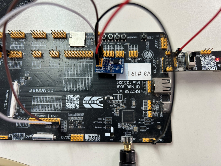
Figure 1. i2c_connect_Diagram
2、Here are the commands in the order:
cpu1 i2c 1 init
[11:45:42.140]发→◇cpu1 i2c 1 init
[11:45:42.145]收←◆cpu1 i2c 1 init
os:I(6720):create shell_handle, tcb=28078db0, stack=[28077188-28078d88:7168], prio=5
$
$cpu1:i2c:I(6178):I2C(1) init ok, baud_rate:400000
cpu1:cli:I(6178):i2c(1) init
cpu1 i2c 1 memory_write 8 50 1//Write 8 bytes of data to EEPROM.
[11:45:43.027]发→◇cpu1 i2c 1 memory_write 8 50 1
[11:45:43.034]收←◆cpu1 i2c 1 memory_write 8 50 1
os:I(7608):create shell_handle, tcb=28078db0, stack=[28077188-28078d88:7168], prio=5
$
$cpu1:cli:I(7066):i2c(1) memory_write buf_len:8
- cpu1 i2c 1 memory_read 8 50 1 //Read 8 bytes of data from EEPROM.
3、Timing Diagram
Write Timing Diagram
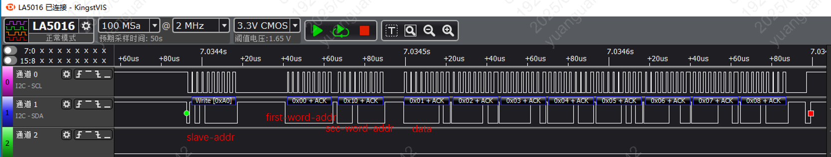
Figure 2. i2c_wr_Sequence_ZD24C128A
read Timing Diagram
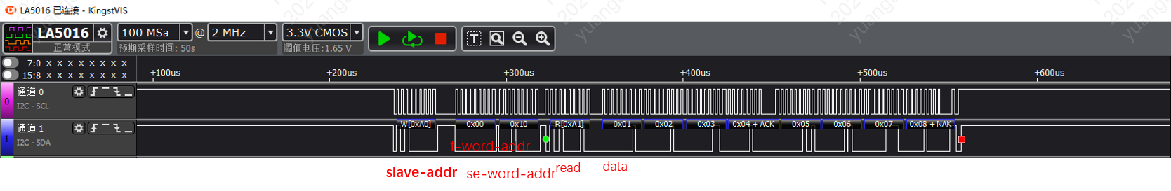
Figure 3. i2c_rd_Sequence_ZD24C128A
The steps for executing demo2 are as follows:
1、Prepare the EEPROM module with the model number FM24C04B and use the I2C1 connection method as follows:
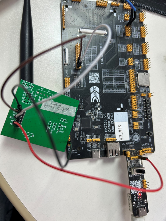
Figure 4. i2c_connect_diagram
2、Here are the commands in the order:
cpu1 i2c 1 init
[16:44:55.619]发→◇cpu1 i2c 1 init
[16:44:55.622]收←◆cpu1 i2c 1 init
os:I(3120):create shell_handle, tcb=28078db0, stack=[28077188-28078d88:7168], prio=5
$
$cpu1:i2c:I(2984):I2C(1) init ok, baud_rate:400000
cpu1:cli:I(2984):i2c(1) init
cpu1 i2c 1 memory_write 8 50 0//Write 8 bytes of data to EEPROM.
[16:44:58.285]发→◇cpu1 i2c 1 memory_write 8 50 0
[16:44:58.292]收←◆cpu1 i2c 1 memory_write 8 50 0
os:I(5788):create shell_handle, tcb=28078db0, stack=[28077188-28078d88:7168], prio=5
$
$cpu1:cli:I(5652):i2c(1) memory_write buf_len:8
- cpu1 i2c 1 memory_read 8 50 0 //Read 8 bytes of data from EEPROM.
3、Timing Diagram
Write Timing Diagram
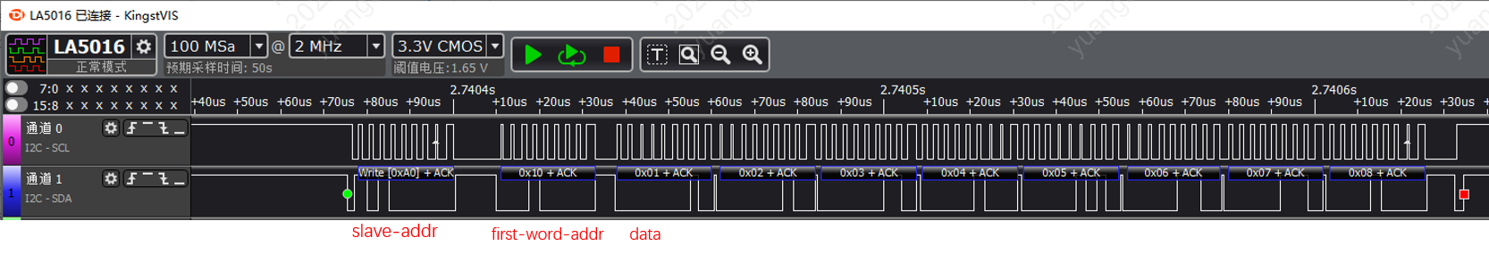
Figure 5. i2c_wr_Sequence_FM24C04B
Read Timing Diagram
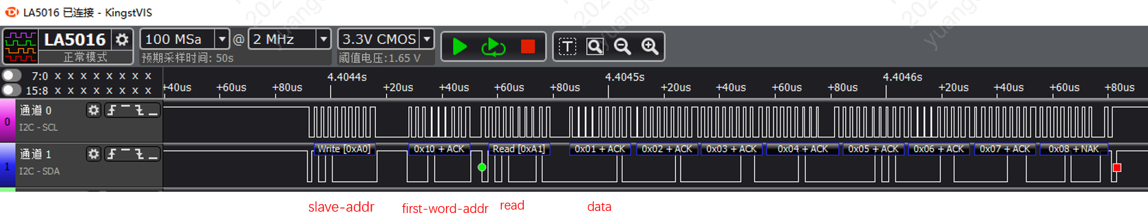
Figure 6. i2c_rd_Sequence_FM24C04B
Note
Note: The dev_addr 50 in the memory_write command is in hexadecimal, because the i2c driver will shift the dev_addr one bit to the left. Therefore, the dev_addr passed in needs to be shifted one bit to the right from the actual dev_addr of ZD24C128A (1010b).