PWM
PWM Introduction
Pulse Width Modulation (PWM) is a technology that implements analog voltage control using digital methods. It achieves this by modulating the width of a series of pulses to produce the desired waveform (including shape and amplitude), digitally encoding the analog signal level. In other words, it regulates the change in signal, energy, etc. by adjusting the change in duty cycle, which is the percentage of time the signal is at a high level within a cycle. For example, a square wave has a duty cycle of 50%.
The BK7258 has two PWM controllers, PWM0 and PWM1, each with three TIM timers, and each timer has two channels.
Taking PWM0 as an example, the relationship between TIM and PWM channels is as follows:
TIM Index |
Channel Index |
|---|---|
TIM1 |
0 |
1 |
|
TIM2 |
2 |
3 |
|
TIM3 |
4 |
5 |
Therefore, each PWM controller has 6 channels, and the BK7258 supports a total of 12 channels, corresponding to the software’s PWM_ID_0 to PWM_ID_11.
Operation Modes
Independent Output Mode
Complementary Output Mode
Input Capture Mode
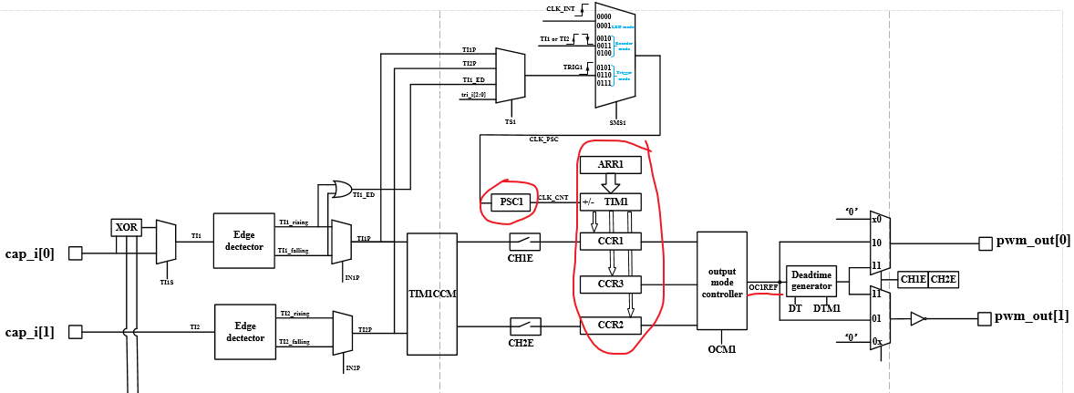
Functional Block Diagram
Clock Source
- The PWM controller has two clock sources to choose from:
clk_32K
XTAL
These can be configured through SYSTEM_REG0x8.
PSC
Prescaler, which divides the input clock (clk_32K or XTAL) and outputs CLK_CNT to drive the counter TIM.
The PSC setting can be configured through PWM_REG_0xE, allowing for a division ratio of 1-256.
For example:
When the clock source is chosen as XTAL=26MHz and PSC1 is set to 25, the clock frequency of counter TIM1 is 1MHz, and if the counter increments by 1, it increments by 1us.
CCR
When the value of the counter CNT equals the value of the compare register CCR, the polarity of the output reference signal OCxREF will change, and a CCxI interrupt will be generated, setting the corresponding flag bit CCxIF (in the REG_0x8 register).
After this, OCxREF will undergo a series of controls before outputting the PWM signal.
The BK7258 has three CCRs for each TIM, which means that the signal polarity can be flipped three times within a cycle. Specifically:
CCR1, CCR2, and CCR3 (REG_0x15-REG_0x17) correspond to TIM1
CCR4, CCR5, and CCR6 (REG_0x18-REG_0x1a) correspond to TIM2
CCR7, CCR8, and CCR9 (REG_0x1b-REG_0x1d) correspond to TIM3
When used in PWM output mode, the duty cycle of the output square wave signal is determined by the CCR.
Note
CCRx must be set to a value greater than 1.
ARR
The Auto-Reload Register (ARR) is used to store the value compared with the counter CNT, and can be understood as the end value of the counter’s count.
The frequency of the PWM output square wave signal is determined by the value of ARR.
Deadtime Generator
Based on the generated reference signal OCxREF, dead time can be inserted to generate two complementary output signals.
The size of the dead time is specifically configured by the DTx bits in REG_0x1E.
PWM Output Mode
Output Single-Channel Square Wave Signal
For each group of PWM, only one of the adjacent channels can be independently output ((0,1) adjacent, (2,3) adjacent, (4,5) adjacent). Simultaneous output will cause mutual interference.
Output Complementary PWM with Dead Time
Regarding complementary output, it can be divided into two modes: hardware-implemented complementary mode and software-complementary mode:
Hardware: Each group of PWM can implement 3 complementary outputs, as shown in the table in the overview. Only PWMx’s CH0 and CH1, CH2 and CH3, and CH4 and CH5 can be configured as complementary outputs, with corresponding dead time registers available for configuration. This method is more precise, but the channels are fixed.
Software: Using PWM0’s CH0, CH2, CH4 and PWM1’s CH0, CH2, CH4, any two channels can be combined to form a complementary output. This method implements the complementary function through software, making it more flexible, but the precision is not as good as the hardware implementation.